Every major semiconductor research center worldwide is searching for a successor semiconductor process technology for complementary metal oxide semiconductors (CMOS)—the only game in town today, but doomed to obsolescence by the laws of atomic-scale physics beyond the 3nm node.
There are dozens of possible successors to CMOS, but only one worldwide center of excellence benchmarking them against each other: the Nanoelectronics Research Initiative (NRI), sponsored by the non-profit Semiconductor Research Corporation, which is underwritten by 2,400 academic researchers and 3,100 industry liaisons at companies including Analog Devices, ARM, Global Foundries, IBM, Intel, Mentor, Micron, Microsoft, Mubadala, NXP, Qualcomm, Samsung, SK Hynix, Texas Instruments, Taiwan Semiconductor Manufacturing Co., Tokyo Electron, and Veeco Instruments.
NRI has narrowed the field of possible CMOS successors to five different types of bit carriers—charge (as used by CMOS today), electric dipoles (as in ferroelectric field-effect transistors/FeFETs), magnetic dipoles (as in all-spin logic and spin-wave devices), orbital state (as in Bilayer-pseudo-Spin Field Effect Transistors/BiSFETs), and strain (as in Piezoelectric FETs).
The general conclusion of the NRI is that "Spintronic devices are slower than charge-based devices because of the limited ferromagnet switching speed and domain wall propagation speed. [However,] voltage-controlled spintronics devices are more energy efficient than current-driven ones. [In addition,] spintronic devices show great performance in neuromorphic computing circuits [based on the deep-learning paradigm], which differ significantly from their results in Boolean circuits, such as a 32-bit ALU [arithmetic logic unit]. This indicates that [post-CMOS] devices need to be complemented with novel circuit [architectures, such as neuromorphic], to achieve their full potential."
Said NRI executive director An Chen, "NRI's follow-on program nCORE (nanoelectronic COmputing REsearch) continues to emphasize that basic material, device, and interconnect research is essential for beyond-CMOS technologies. Holistic approaches combining novel devices and architectures (as well as their co-optimization) are critical for beyond-CMOS research. We also need to be mindful of educational aspects. We need more, not fewer, talented researchers to explore basic research in the post-CMOS era."
The details of NRI's benchmarking methods and results are available as Matlab files at https://nanohub.org/tools/nribench/browser/trunk/src.
Use of CMOS likely will fade during the next decade, with last-ditch efforts to prolong its use including three-dimensional (3D) stacking, gate-all-around silicon nanowire FETs, heterogeneous architectures (using novel accelerators with CPUs), and the use of mixed materials (such as gallium arsenide transistor channels atop silicon substrates), along with extreme ultra-violet (EUV) lithography, and innovative chip-layout schemes, according to both NRI and the European Union's semiconductor innovation hub IMEC.
However, while the post-CMOS era to follow was once predicted to switch from silicon to carbon materials such as graphene and nanotubes, the consensus at NRI and IMEC is rather that the most promising post-CMOS paradigms will turn to quantum effects, such as tunneling FETs and spintronic devices.
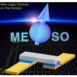
For instance, Intel recently announced proof-of-concept success, in collaboration with the University of California, Berkeley and the Lawrence Berkeley National Laboratory, at designing a spintronic architecture that aims to achieve optimal performance among post-CMOS devices. It is called a magneto-electric spin-orbit (MESO) chip and is up to 100 times more energy efficient, up to 30 times faster, uses a fifth of the voltage, is five times denser, and achieves ultra-low sleep state power, compared to CMOS.
Said Intel Senior Fellow Ian Young, director of the Exploratory Integrated Circuits group in the company's Technology and Manufacturing Group, "We are looking for revolutionary, not evolutionary, approaches for computing in the beyond-CMOS era. MESO is built around low-voltage interconnects and low-voltage magneto-electrics. It brings together quantum material innovations with computing. We are excited about the progress we have made and are looking forward to future demonstrations of reducing the switching voltage even further toward its potential."
In the recent paper Scalable energy-efficient magnetoelectric spin–orbit logic, the researchers describe how room-temperature quantum materials that are both ferroelectric and magnetic (namely bismuth, iron, and oxygen, as BiFeO3) achieve these post-CMOS qualities. Since the magnetic and electrical properties of the material are coupled, it is possible to use electricity to change the magnetic spin, and likewise to efficiently read out the magnetic state of the multiferroic spin-orbit using electricity. MESO will require the development of unique materials and techniques, but because it utilizes spin-orbit transduction of electrons, it could enable revolutionary new types of both computing devices and circuit architectures, according to the researchers.
"MESO is a device built with room-temperature quantum materials," said Sasikanth Manipatruni, senior staff scientist and director of Intel's Science and Technology Center on Functional Electronics Integration and Manufacturing. "It is an example of what is possible, and hopefully triggers innovation across industry, academia and the national labs. A number of critical materials and techniques are yet to be developed to allow these new types of computing devices and architectures."
Unlike storing qubits, as with quantum computers made by D-Wave, IBM, Google, and Microsoft, the quantum effects realized by Intel's MESO materials store conventional bits using topological properties that enable lowering the switching voltage from the three volts commonly used by CMOS to the 500 millivolts used by today's MESO, with predictions that further optimization could reduce switching voltage to as low as 100 millivolts. Such low voltages are so far impossible for CMOS, and could greatly lower the power requirements for all post-CMOS chips.
Topological multi-ferroic and spin-orbit materials like MESO also possess unique quantum properties, according to the researchers, exhibiting more than one "collective state" simultaneously, in a manner similar to superposition in superconductors. In addition, these topological materials exhibit a spin-orbit effect that makes it easy, and extremely energy-efficient, to read out bits, according to the researchers. The quantum effect called spin-orbit coupling produces an energy-efficient current that identifies the electron spin direction, and thus the value of the bit.
R. Colin Johnson is a Kyoto Prize Fellow who has worked as a technology journalist for two decades.

Join the Discussion (0)
Become a Member or Sign In to Post a Comment